. DOI: 10.1038/s41377-024-01477-3")
The characteristic measurement of silicon-based transistors is approaching the theoretical restrict, which places ahead increased necessities for the atomic degree manufacturing of semiconductors. The fundamental concept of atomic degree manufacturing is to course of and manipulate issues with atomic degree precision, which is able to vastly scale back the facility consumption of the chip and obtain an enormous enhance within the chip’s arithmetic energy.
2D supplies are anticipated to deal with the challenges confronted by conventional silicon-based semiconductor units. The p-n junction is the essential unit of optoelectronic units within the data age.
Earlier research have proven that 2D vertical p-n junctions might be ready merely no matter lattice mismatch. Nevertheless, because of the van der Waals hole in interfaces and the impurities launched within the stacking course of, 2D vertical p-n junctions will scale back the provider mobility.
The 2D lateral p-n junction can successfully resolve these issues. Due to this fact, learn how to notice the development of high-quality 2D lateral p-n junction is essential for the sensible software of 2D semiconductors.
Ion implantation method is a mature doping methodology for establishing p-n junctions within the conventional semiconductor trade, which has the deserves of controllable doping focus and depth, plentiful doping parts, uniform doping space and non-polluting doping course of.
Nevertheless, because of the excessive power of incident ions (tens of keV), the standard ion implantation method will trigger injury and even penetrate the atomically skinny 2D supplies throughout the implantation course of, leading to machine failure. Due to this fact, it’s tough to immediately modulate {the electrical} and optical properties of 2D supplies utilizing standard ion implantation.
In a paper printed in Mild Science & Functions, a group of scientists, led by Professor Xiangheng Xiao from College of Physics and Know-how, Key Lab of Synthetic Micro- and Nano-Constructions of Ministry of Training, Wuhan College, Wuhan, China, has developed a low-energy ion implantation system for establishing 2D lateral p-n homojunction.
Low-energy ion implantation method inherits the benefits of the standard ion implantation method. It has a decrease ion power and shallower implantation depth, which is predicted to deal with the issue that conventional ion implantation strategies can’t be immediately utilized to modulate the efficiency of 2D supplies.
Though a number of teams have performed analysis on low-energy ion implantation, they’ve primarily targeted on the microscopic characterization and defect modulation. Thus far, there’s a lack of analysis on utilizing low-energy ion implantation to realize patterned p-type doping on 2D supplies to utterly reverse their conductivity varieties and assemble lateral p-n homojunctions.
By exactly modulating the implantation dose, the conductivity kind of the WS2 flake is efficiently modulated, which might be transformed from n-type to bipolar and even p-type. The universality of this methodology can also be demonstrated by extending it to different 2D semiconductors. As well as, the photodetector based mostly on WS2 lateral p-n homojunction reveals passable self-powered photodetection functionality.
This work supplies an efficient methodology for controllable doping of 2D supplies and promotes the sensible software of 2D supplies.
The authors used the low-energy ion implantation method to immediately implant nitrogen ions into the few-layer WS2, and realized exact modulation of WS2 conductive kind by controlling the implantation dose of low-energy nitrogen ions.
-
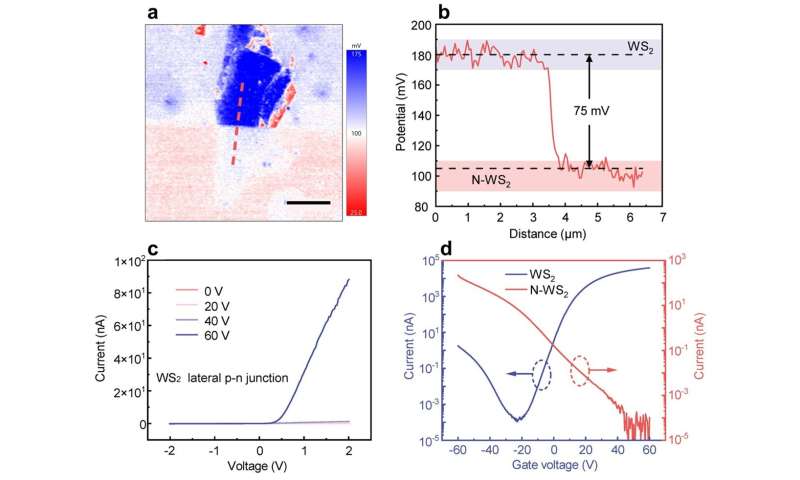
The measurement outcomes of KPFM and electrical efficiency on WS2 lateral p-n homojunction. Credit score: Mild: Science & Functions (2024). DOI: 10.1038/s41377-024-01477-3
-

The photoelectric efficiency of WS2 lateral p-n homojunction photodetector. Credit score: Mild: Science & Functions (2024). DOI: 10.1038/s41377-024-01477-3
“By growing the implantation dose, the conductive kind of WS2 might be modified from n-type to bipolar- and even p-type. On the ion implantation dose of 1×10¹⁴ ions cm-2, the present on/off ratio of N-WS2 FET can attain 3.9×10⁶. The efficiency of N-WS2 FET doesn’t deteriorate considerably after three months, indicating the soundness of the doping methodology,” mentioned the researchers.
“Low-energy nitrogen ion implantation has been prolonged to different typical n-type two-dimensional steel chalcogenides supplies, similar to WSe2, MoS2 and SnS2. Their conductivity varieties have been efficiently reworked from n-type to p-type, demonstrating the universality of the strategy,” they added.
By combining low-energy ion implantation method with lithography method, the authors realized patterned doping of 2D supplies. The WS2 lateral p-n homojunction was efficiently fabricated.
“Kelvin probe power microscopy characterizes that there’s an apparent floor potential distinction within the junction area, and demonstrates the feasibility of establishing lateral p-n homojunction with patterned doping by this methodology. The p-n junction reveals vital photovoltaic impact underneath illumination, and reveals passable self-powered photodetection potential underneath totally different wavelength lasers.”
“Below 532-nm laser illumination at 1.7 mW cm-2, the self-powered photodetector based mostly on this p-n junction can obtain an open-circuit voltage of 0.39 V, responsivity and detectivity of roughly 35 mA W-1 and 9.8×10¹⁰ Jones.”
The researchers say, “This doping methodology appropriate with built-in circuits reveals an enormous software potential on modulating the efficiency of 2D semiconductor units, and supplies a dependable technique for selling the sensible software of 2D supplies.”
Extra data:
Yufan Kang et al, Spatially selective p-type doping for establishing lateral WS2 p-n homojunction by way of low-energy nitrogen ion implantation, Mild: Science & Functions (2024). DOI: 10.1038/s41377-024-01477-3
Supplied by
Wuhan College
Quotation:
Low-energy ion implantation permits 2D lateral p-n junction building (2024, September 2)
retrieved 2 September 2024
from https://phys.org/information/2024-09-energy-ion-implantation-enables-2nd.html
This doc is topic to copyright. Aside from any honest dealing for the aim of personal examine or analysis, no
half could also be reproduced with out the written permission. The content material is offered for data functions solely.