| Aug 05, 2024 |
|
(Nanowerk Information) Clear electronics are already offering dependable companies in some purposes. For example, they are often discovered as ultra-thin layers for contact shows or as clear movies with printed antennas for cell communications. Nonetheless, OLED microdisplays haven’t been clear up to now.
|
|
As a part of the HOT venture (“Excessive-performance clear and versatile micro-electronics for photonic and optical purposes”), OLED microdisplays with 20% transparency had been developed. The know-how has now been superior additional, and for the primary time, 45% transparency has been achieved in a CMOS OLED microdisplay.
|
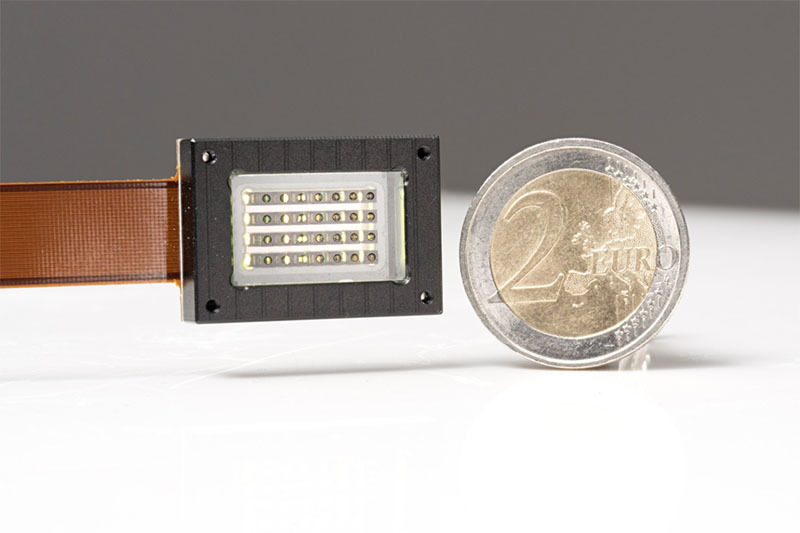 |
| Clear OLED microdisplay system. (Picture: Fraunhofer IPMS)
|
What causes this enchancment?
|
|
The OLED-on-silicon know-how makes use of a silicon backplane that accommodates your entire lively matrix drive electronics for the pixels. The natural frontplane is monolithically built-in on the topmost metallization layer, which concurrently serves because the drive contact for the natural light-emitting diode. The second connection of the OLED is fashioned by a semi-transparent prime electrode shared by all pixels.
|
|
The pixel circuitry relies on silicon CMOS know-how and requires a number of steel layers to attach the transistors embedded within the substrate. These steel connections are made from aluminum or copper. Moreover, the optical construction of the OLED requires a extremely reflective backside electrode to make sure excessive optical effectivity upwards. These two facets consequence within the pixels themselves not being clear.
|
|
“A clear microdisplay, nevertheless, might be realized by means of a spatially distributed design of this primary pixel construction, creating clear areas between the pixels and minimizing column and row wiring,” explains Philipp Wartenberg, group chief of IC and system design at Fraunhofer IPMS, “additional optimization of the OLED layers, for instance by avoiding OLED layers within the clear areas, introducing anti-reflective coatings, and redesigning the wiring additionally contributes to rising transparency.”
|
 |
| Clear OLED microdisplay. (Picture: Fraunhofer IPMS)
|
|
There are two elementary strategies to attain semi-transparency in optical methods:
|
- Pixel strategy: This includes creating clear areas between particular person pixels.
- Cluster strategy: This technique teams a number of pixels into a bigger, non-transparent cluster. Bigger clear areas are created between these clusters.
|
|
Each approaches are related for various purposes in apply. The pixel strategy is appropriate, for instance, for picture overlay inside a posh optical system, the place the picture is inserted between different picture planes.
|
|
The cluster strategy is especially appropriate for augmented actuality (AR) purposes, corresponding to in knowledge glasses, the place the pixel clusters are mixed right into a uniform digital picture utilizing a micro-optic over every cluster. The clear areas between the clusters stay unaffected by the optics, permitting a transparent view of the actual surroundings.
|
|
The know-how for clear microdisplays was developed to help each strategies. The microdisplay introduced at IMID showcases the cluster strategy with a brand new AR optic.
|
Optical Method
|
|
The optical mixture of the person pixel clusters right into a uniform digital picture was realized by means of a microlens array. The optics had been designed to allow a setup near the attention with an identical distance to the attention as common corrective glasses.
|
|
Fraunhofer IPMS at IMID 2024: Sales space: No. 38
|